- 您现在的位置:买卖IC网 > Sheet目录515 > SIR158DP-T1-GE3 (Vishay Siliconix)MOSFET N-CH D-S 30V 8-SOIC
New Product
SiR158DP
Vishay Siliconix
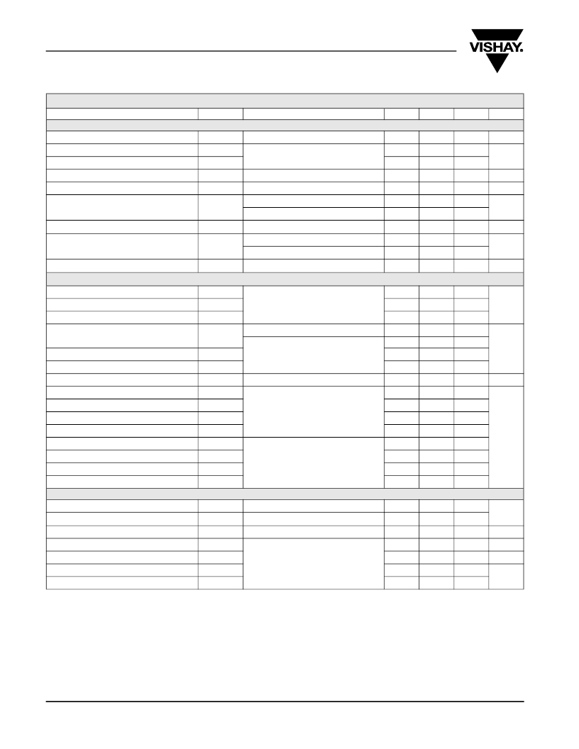
SPECIFICATIONS T J = 25 °C, unless otherwise noted
Parameter
Symbol
Test Conditions
Min.
Typ.
Max.
Unit
Static
Drain-Source Breakdown Voltage
V DS Temperature Coefficient
V GS(th) Temperature Coefficient
V DS
Δ V DS /T J
Δ V GS(th) /T J
V GS = 0 V, I D = 250 μA
I D = 250 μA
30
24
- 6.6
V
mV/°C
Gate-Source Threshold Voltage
V GS(th)
V DS = V GS , I D = 250 μA
1.2
2.5
V
Gate-Source Leakage
Zero Gate Voltage Drain Current
On-State Drain Current a
I GSS
I DSS
I D(on)
V DS = 0 V, V GS = ± 20 V
V DS = 30 V, V GS = 0 V
V DS = 30 V, V GS = 0 V, T J = 55 °C
V DS ≥ 5 V, V GS = 10 V
30
± 100
1
10
nA
μA
A
Drain-Source On-State Resistance a
Forward Transconductance a
R DS(on)
g fs
V GS = 10 V, I D = 20 A
V GS = 4.5 V, I D = 20 A
V DS = 10 V, I D = 20 A
0.00145
0.00185
100
0.0018
0.0023
Ω
S
Dynamic
b
Input Capacitance
C iss
4980
Output Capacitance
Reverse Transfer Capacitance
C oss
C rss
V DS = 15 V, V GS = 0 V, f = 1 MHz
915
495
pF
Total Gate Charge
Gate-Source Charge
Q g
Q gs
V DS = 15 V, V GS = 10 V, I D = 20 A
V DS = 15 V, V GS = 4.5 V, I D = 20 A
87
41.5
10.6
130
63
nC
Gate-Drain Charge
Q gd
13.8
Gate Resistance
R g
f = 1 MHz
0.2
0.7
1.4
Ω
Turn-On Delay Time
t d(on)
16
30
Rise Time
Turn-Off Delay Time
t r
t d(off)
V DD = 15 V, R L = 1.5 Ω
I D ? 10 A, V GEN = 10 V, R g = 1 Ω
9
44
18
80
Fall Time
Turn-On Delay Time
t f
t d(on)
9
28
18
50
ns
Rise Time
Turn-Off Delay Time
Fall Time
t r
t d(off)
t f
V DD = 10 V, R L = 1 Ω
I D ? 10 A, V GEN = 4.5 V, R g = 1 Ω
36
47
16
70
90
30
Drain-Source Body Diode Characteristics
Pulse Diode Forward Current
Continuous Source-Drain Diode Current
a
I S
I SM
T C = 25 °C
60
80
A
Body Diode Voltage
Body Diode Reverse Recovery Time
Body Diode Reverse Recovery Charge
Reverse Recovery Fall Time
Reverse Recovery Rise Time
V SD
t rr
Q rr
t a
t b
I S = 4 A
I F = 10 A, dI/dt = 100 A/μs, T J = 25 °C
0.71
29
22
15
14
1.1
45
33
V
ns
nC
ns
Notes:
a. Pulse test; pulse width ≤ 300 μs, duty cycle ≤ 2 %.
b. Guaranteed by design, not subject to production testing.
Stresses beyond those listed under “Absolute Maximum Ratings” may cause permanent damage to the device. These are stress ratings only, and functional operation
of the device at these or any other conditions beyond those indicated in the operational sections of the specifications is not implied. Exposure to absolute maximum
rating conditions for extended periods may affect device reliability.
www.vishay.com
2
Document Number: 64730
S09-0318-Rev. A, 02-Mar-09
发布紧急采购,3分钟左右您将得到回复。
相关PDF资料
SIR19-21C/TR8
LED IR GAA1AS WATER CLR FLAT SMD
SIR19-315/TR8
LED IR A1GAAS WATER CLR MINI SMD
SIR204-A
LED IR 3MM GAA1AS BLUE RADIAL
SIR204C
LED IR 3MM GAA1AS WATER CLR AXL
SIR323-5
LED IR 5MM WATER CLEAR RADIAL
SIR333-A
LED IR 5MM WATER CLEAR RADIAL
SIR383C
LED IR 5MM BLUE WATER CLEAR AXL
SIR383
LED IR 5MM BLUE WATER CLEAR AXL
相关代理商/技术参数
SIR164DP-T1-GE3
功能描述:MOSFET 30V 50A 69W 2.5mohm @ 10V RoHS:否 制造商:STMicroelectronics 晶体管极性:N-Channel 汲极/源极击穿电压:650 V 闸/源击穿电压:25 V 漏极连续电流:130 A 电阻汲极/源极 RDS(导通):0.014 Ohms 配置:Single 最大工作温度: 安装风格:Through Hole 封装 / 箱体:Max247 封装:Tube
SIR166DP
制造商:VISHAY 制造商全称:Vishay Siliconix 功能描述:N-Channel 30-V (D-S) MOSFET
SIR166DP-T1-GE3
功能描述:MOSFET 30V 40A N-CH MOSFET RoHS:否 制造商:STMicroelectronics 晶体管极性:N-Channel 汲极/源极击穿电压:650 V 闸/源击穿电压:25 V 漏极连续电流:130 A 电阻汲极/源极 RDS(导通):0.014 Ohms 配置:Single 最大工作温度: 安装风格:Through Hole 封装 / 箱体:Max247 封装:Tube
SIR168DP-T1-GE3
功能描述:MOSFET 30V 40A 34.7W 4.4mohm @ 10V RoHS:否 制造商:STMicroelectronics 晶体管极性:N-Channel 汲极/源极击穿电压:650 V 闸/源击穿电压:25 V 漏极连续电流:130 A 电阻汲极/源极 RDS(导通):0.014 Ohms 配置:Single 最大工作温度: 安装风格:Through Hole 封装 / 箱体:Max247 封装:Tube
SIR17-21C
制造商:EVERLIGHT 制造商全称:Everlight Electronics Co., Ltd 功能描述:Infrared Chip LED
SIR17-21C/TR8
制造商:EVERLIGHT 制造商全称:Everlight Electronics Co., Ltd 功能描述:Infrared Chip LED
SIR172ADP-T1-GE3
制造商:Vishay Semiconductors 功能描述:N-CHANNEL 30-V (D-S) MOSFET - Tape and Reel 制造商:Vishay Intertechnologies 功能描述: 制造商:Vishay Intertechnologies 功能描述:Single N-Channel 30 V 0.0089 O 12.8 nC Power Mosfet - PowerPAK SO-8
SIR172DP
制造商:VISHAY 制造商全称:Vishay Siliconix 功能描述:N-Channel 30-V (D-S) MOSFET
